汽车用开关稳压器提供输入瞬时电压保护
一个简单的方案保护用承受瞬间50V电压。
工程师经常要面对电压稳压器遭遇高于输入供电范围的瞬间高压后,替换稳压器的困难。这个情形通常在汽车应用中,高压交流发电机负载泵瞬变可以产生36到75V的电压,持续长达400ms。设计人员必须在能经受住这样大限度输入电压的稳压器或使用输入保护方案之间做出选择。本设计方案的简单电路提供了利用20V 3MHz稳压器的低成本高效率方法,钳位电池输入端出现瞬间高达50V的电压。用这个电路,设计以相对的低费用实现小型全焊盘,因为随同更低压的器件一起的3MHz工作必须能够承受50V电压。
输入保护器件由Q1、R1、D1、C5和D2的一半组成(图1)。上电时,N沟道MOSFET的Q1源极处于地电压,当R1将电池电压供到门极时,Q1打开。一旦输入电压大于IC1的最小2.74V,LM2734Z稳压器开始工作,其通过D3、D4和CB组成的自举电路充电。然后,D3近似VOUT–VFD(前项压降)的这个自举电压传输到Q1的门源极。电容C5在自举二极管关闭的时间内,维持门极驱动。
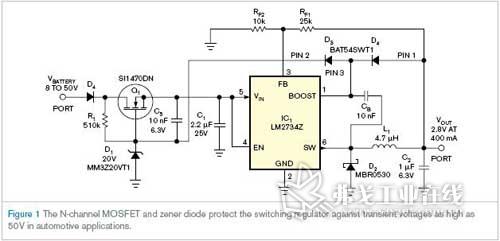
在正常工作的条件下,例如,电池电压为8到18V,D1
Q1 SI1470DN N沟道MOSFET用30V+20V(zener二极管D1电压)漏源极电压(VDS)提供了50V的保护,在2.5V门源极电压处有95mΩ的阻抗,来自高热效的SC70-6封装。对一般应用,稳压器的输出电压不足以完全打开挑选的保护MOSFET,所以可以增加带隔离zener 参考的自举电压,LM2734Z的数据手册见参考文献1。
英文原文:
Automotive switching regulators get input-transient-voltage protection
A simple scheme protects switching regulators against 50V voltage transients in automotive applications.
Kevin Daugherty, National Semiconductor, Novi, MI; Edited by Charles H Small and Fran Granville -- EDN, 1/24/2008
Engineers often face difficult trade-offs when voltage regulators can encounter high-voltage transients that are well above normal input-supply operating ranges. This situation is common in automotive applications in which high-voltage transients from an alternator load dump can produce transients of 36 to 75V for durations as long as 400 msec. Designers must choose between a regulator that can withstand such maximum input voltage or use an input-protection scheme. The simple circuit in this Design Idea provides a highly cost-effective method for clamping an input voltage from a battery input with transients as high as 50V to take advantage of a 20V, 3-MHz regulator. With this circuit, your design can achieve a small total footprint with relatively low cost because of the 3-MHz operation along with lower voltage components than might otherwise be necessary to withstand 50V. #p#副标题#e#
Input-protection components consist of Q1, R1, D1, C5, and one-half of D2 (Figure 1). At start-up, N-channel MOSFET Q1’s source is at ground potential and turns on when R1 applies the battery voltage to the gate. Once the input voltage is above the minimum of 2.74V on IC1, the LM2734Z regulator starts switching, which charges the bootstrap circuit comprising D3, D4, and CB. This bootstrap voltage of approximately VOUT–VFD (forward
Under normal operating conditions, for example, the battery voltage is 8 to 18V, D1 does not limit conduction of Q1, and the gate voltage tracks approximately 2.5V above the input-supply voltage for a low voltage drop from the battery voltage to the input voltage of the LM2734Z. However, when the input voltage increases above the threshold that D1 sets, the input voltage to the LM2734Z regulates to the zener voltage (VZ) of D1 minus the threshold voltage of Q1, or approximately 20–2V=18V, well below the 24V absolute maximum of the LM2734Z. Selecting Q1 requires careful consideration of maximum input voltage, gate-to-source-voltage threshold, and power dissipation under both steady-state and thermal-transient conditions.
Q1, the SI1470DN N-channel MOSFET, provides 50V protection with a drain-to-source voltage (VDS) of 30V+20V (zener diode D1 voltage), has an on-resistance of 95 mΩ at a gate-to-source voltage of 2.5V, and comes in a thermally efficient SC70-6 package. For some applications, the regulator’s output voltage may be insufficient to fully turn on the selected protection MOSFET, so you can increase the bootstrap voltage with a separate zener reference, as the LM2734Z’s data sheet shows (Reference 1).
Reference
“LM2734Z Thin SOT23 1A Load Step-Down DC-DC Regulator,” National Semiconductor.
英文原文地址:











获取更多评论